3D X-DRAMTM
TCAD Simulation Data

3D X-DRAM is a revolutionary 3D DRAM technology based on a floating body cell with a 3D NAND-like cell structure. Neo Semiconductor announced a patented performance boosting Floating Body Cell Mechanism for 3D X-DRAM called Back-gate Channel-depth Modulation (BCM) that can increase data retention by 40,000X and sensing window by 20X. 

Data 1 (High current)

Data 0 (Low current)

neosemic

Technology Computer-Aided Design (TCAD) is utilized to optimize 3D X-DRAM cell structure and operations. The cell is written with data 1 using impact ionization and data 0 using forward bias condition.

TCAD simulation

Write 1 Operation

TCAD simulation shows write 1 operation using impact ionization. Front gate and bit line are applied with 0.7V and 0.6V, respectively, to trigger impact ionization to inject electric holes into the floating body in 3 ns. Back gate is applied with -1V to attract electric holes. These holes stored in the floating body will increase body potential to increase the cell’s read current. This state represents data 1.

TCAD Simulation

TCAD simulation

Write 0 Operation

TCAD simulation shows write 0 operation using forward bias condition. Front gate and back gate are both applied with 1V to couple up the potential of the floating body. Bit line is applied with 0V to create a forward bias current to extract electric holes from the floating body to the bit line in 1 ns. This will reduce the body potential to reduce the cell’s read current. This state represents data 0.

Sensing Margin

Simulation

TCAD simulations show the sensing margin of 3D X-DRAM is higher than 20 uA. This high margin allows the cell to achieve high read speed, long data retention time, and reduce data error rate.

Retention Time

Simulation (85oC)

TCAD simulation shows 3D X-DRAM cell’s dual-gate structure can effectively increase the retention time to be longer than 100 ms under 85 degrees C. This meets DRAM requirement.

neosemic

Write Condition

Simulation

TCAD simulations show the required voltage for write 1 operation is below 0.4V. This can greatly reduce hot-carrier degradation to improve cell endurance. Based on research, 3D X-DRAM can achieve more than 1016 endurance cycles to meet DRAM requirement.

TCAD Simulation Results

for 3D X-DRAM Cell Characteristics
neosemic
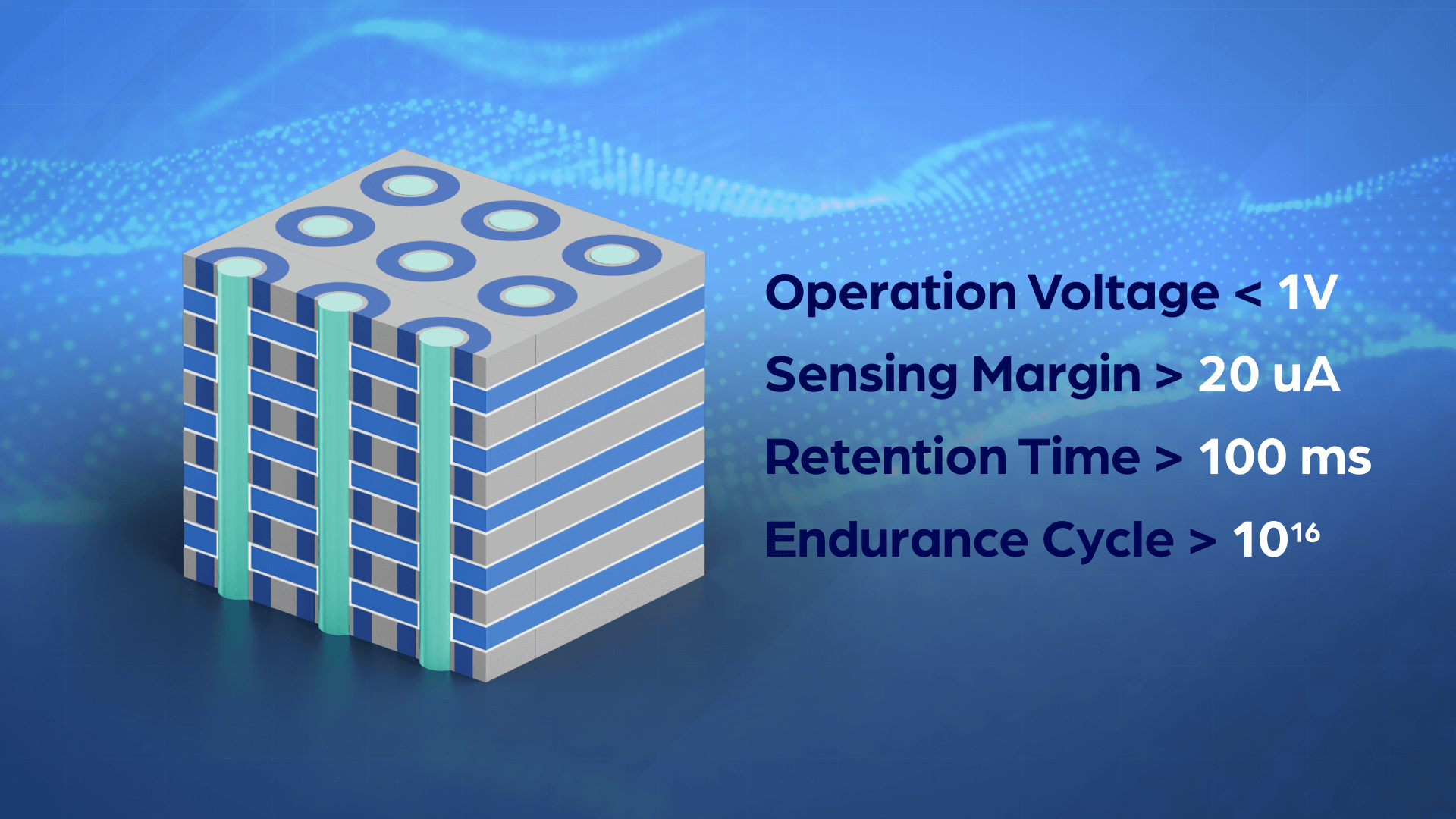
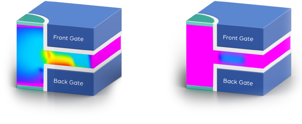
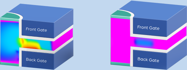
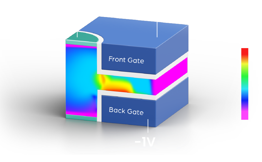
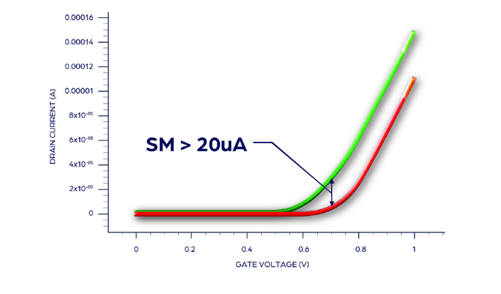
The TCAD simulation results show 3D X-DRAM’s unique cell structure and novel operation mechanism can successfully solve traditional 2D Floating Body Cell’s problems and achieve excellent performances. With its high-density 3D NAND-like array, 3D X-DRAM provides an ultimate solution for future DRAM and AI applications.

Looking for more information?