X-DRAMTM
World’s Lowest
Power Consumption
Next Gen Architecture for DRAM
Dynamic Random-Access Memory (DRAM) is used to support processors, making DRAM usage common in electronic devices. However, processor speeds have grown at higher rates than memory speeds across multiple generations and the resulting “performance gap” widens annually. Power-sensitive environments like cloud data centers increasingly rely on higher-power processors to meet performance requirements but this leaves less power available for memory.
Adopting X-DRAM architecture reduces power consumption, lowers latency, and increases throughput to overcomes these and other challenges that occur when using conventional DRAM. This results in higher performance for business systems (e.g., servers), longer battery life for mobile devices (e.g., smartphones), more capabilities for edge computing devices (e.g., routers), and new deployment options for Internet of Things objects (e.g., gateways).
X-DRAM™ is the property of NEO Semiconductor, Inc.
Architecture Comparison
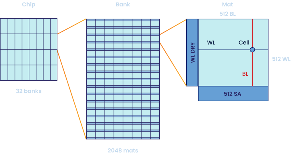
DRAM chips include multiple banks that contains thousands of mats and millions of cells arranged in a matrix of rows and columns called an array. Each mat includes 512 word lines (WL) and 512 bit lines (BL) with a memory cell formed at each intersection. Sense amplifier (SA) circuits are used to detect the current of a cell and convert that to a digital data of 1 or 0.
X-DRAMTM
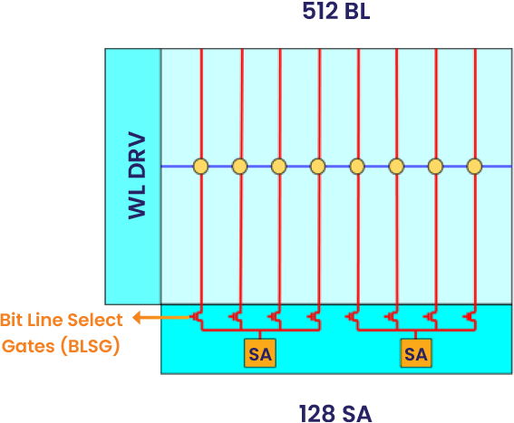
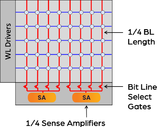
X-DRAM connects one Sense Amplifier (SA) to four Bit Lines (BL) through four Bit Line Select Gates (BLSG).
Conventional
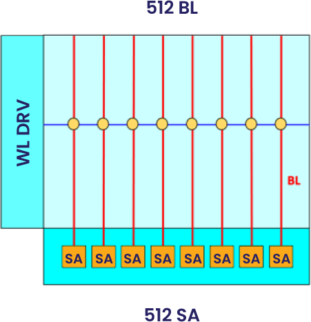
Conventional DRAM connects one Sense Amplifier (SA) to a Bit Line (BL) directly.
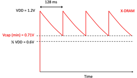
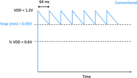
85% Lower Refresh Power
X-DRAMTM
Conventional
400% Higher Refresh Data Throughput
X-DRAMTM
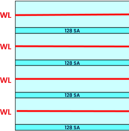
X-DRAM allows four word lines (WL) to perform read and write operations in parallel, increasing data throughout by 400% during refresh operation.
Conventional
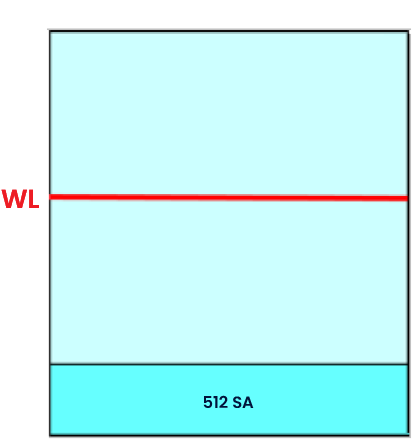
Conventional DRAM performs read and write operations using one word line at a time.
50% Lower Activation Latency
X-DRAMTM
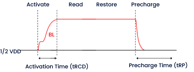
X-DRAM reduces bit line length and capacitance, and this reduces activation time (tRCD) and precharge time (tRP).
Conventional
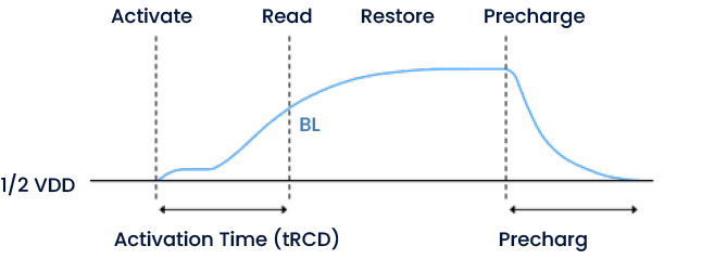
Conventional DRAM uses longer bit line lengths with higher capacitance, increasing activation time (tRCD) and precharge time (tRP).
Other X-DRAMTM Benefits
Faster Performance
Throughput
Lower Voltage
Voltage
Reduced Power
X-DRAM delivers many benefits over conventional DRAM including significant advantages related to faster performance, lower voltage, and reduced power.
X-DRAM™ Application Examples
High-Bandwidth
Memory (HBM)
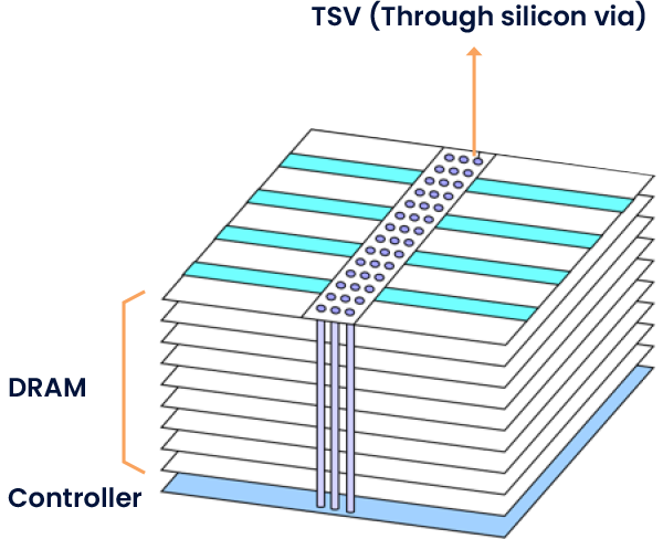
X-DRAM™ significantly reduces data latency and provides ultra-high data throughput to unleash the full potential of High-Bandwidth Memory (HBM).
HBM uses many Through Silicon Via (TSV) to increase I/O bandwidth. However, the HBM data latency remains almost the same when using conventional DRAM because bit line lengths remain the same.
System on Chip
(SoC)
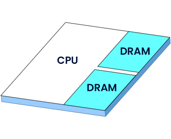
X-DRAM™ significantly reduces data latency and provides ultra-high data throughput to unleash the full potential of System on Chip (SoC) designs.
SoC uses on-board memory to enhance performance. However, performance is limited by the available latency, throughput, and power consumption of conventional DRAM.
