QLC 3D NAND flash has already found many applications due to its higher density and lower price than other NAND types. However, a serious limitation is that QLC has relatively low performance, especially write speed. NEO Semiconductor has developed a new architecture called X-NAND, which can increase QLC NAND’s random read/write speed by 3X and sequential read/write throughput by 15-30X. That results in QLC NAND with read/write performance comparable to SLC NAND. X-NAND architecture can produce the high-speed, low-cost solution required by such emerging applications as AI, 5G, real-time analysis, VR/AR, and cybersecurity. X-NAND architecture can be applied to all generations of flash memory (e.g., SLC, MLC, TLC, QLC, PLC). The X-NAND architecture enables NAND flash to be readily integrated into ultra-high-bandwidth 3D NAND integrated chips.
X-NAND (trademark pending) is the property of NEO Semiconductor, Inc.
More Planes = Faster Speed
X-NANDTM
3X
Random
R/W Speed
20X
Sequential
Write Speed
30X
Sequential
Read Speed
0%
Cost
Increase
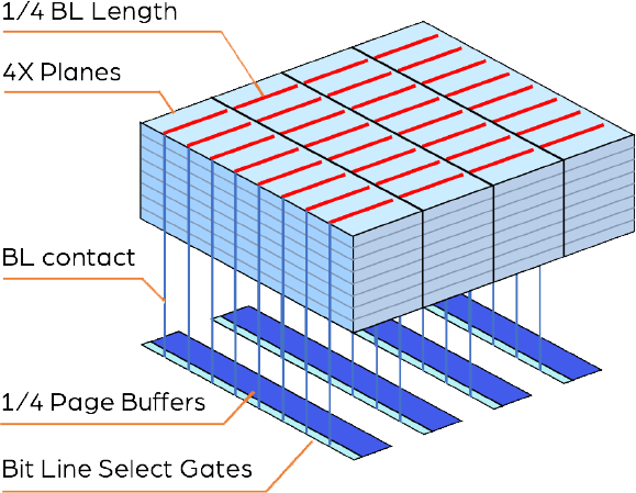
X-NAND architecture divides the array into 16-64 planes (Y-direction) with the same or less page buffers than the conventional, and providing ultra-high speed without increasing the die size.
Conventional NAND
Conventional 3D NAND flash memory only has 2-4 planes (Y-direction) due to the die size only being able to fit 32-64KB of page buffers. The huge capacitance of the long bit lines causes very slow speed.
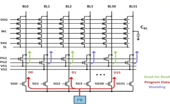
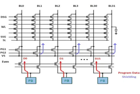
Single Buffer Multiple Bit Line (SBMB) Operations
X-NAND architecture allows one page buffer to perform read and write operations to 16 or more-bit lines. This increases the number of planes in Y-direction to 16 times or more without increasing the number of total page buffers. As a result, the read and write data throughputs are increased by 16 times. In addition, because the bit line length and capacitance are reduced to 1/16, the random read speed and program-verification speed are significantly increased. The bit line power consumption is also reduced to 1/16.
X-NAND™
Conventional NAND
SLC/QLC Parallel Programming
X-NAND’s unique SLC/QLC Parallel Programming allows the data to be programmed to QLC pages at SLC speed for the entire memory capacity. This also solves the conventional NAND’s SLC cache full problem.
No More 'SLC Cache Full' Problem
When the conventional SLC cache is full for traditional NAND, the data will be directly written to QLC cells, and the speed will be dropped to about 12%. X-NAND solves this problem and provides an excellent solution for heavy-write systems such as data centers with NAS systems.
1/16 Bit
Line Power Consumption
X-NAND’s bit line capacitance is only 1/16 of the conventional NAND’s. Therefore, the bit line’s power consumption for read and write operations can be reduced by 1/16. This significantly increases the battery life for smartphones, tablets, and IoT devices.
Conventional NAND
16X BL Capacitance
X-NAND™
1X BL Capacitance
4X More Parallelism Per Chip
X-NAND’s 16-64 plane architecture provides high parallelism at the chip level. Compared with the conventional NAND using 2 – 4 planes, one X-NAND chip can provide the same parallelism of 4 – 16 NAND chips. This allows small form-factor packaging such as M.2 and eMMC which has similar performance to large systems with smaller footprint.
Performance
vs. Price
X-NAND architecture provides advantages for both high performance and low cost. This diagram shows the comparison of die size vs. performance for non-CUA (circuit under array) versions. When using 2X-16X planes, the performance can be increased by 2-16 times. The die cost can be reduced by 33% to 0%, respectively. The number of planes can be optimized to maximize the performance and die cost reduction according to the customer’s needs. For CUA versions, the die size is limited by the 3D array, thus the die cost will be the same as the conventional NAND.
X-NANDTM Performance Estimation
Compared with the conventional QLC NAND, X-NAND can increase the random read speed by 3.5 times by reducing the bit line length to 1/16. Because the program-verification time occupies 90% of the program time, this also increases the program speed about 3 times. Increasing the number of planes by 16X further increases the parallel read and write size. With X-NAND, the sequential read speed is increased by 27 times, and the sequential write speed is increased by 14 times.
SLC - PLC Performance Estimation
X-NAND™
NAND
Random Read & Write Performance Comparison Estimation