August 6-8, 2024 Santa Clara Convention Center – CA, USA
Neo Semiconductor Founder & CEO, Andy Hsu, will deliver a keynote presentation on August 6 at 11:45am PT
Innovating the Future of Al Memory
NEO Semiconductor develops breakthrough Al memory technologies - including X-SRAMTM, 3D X-DRAMTM, and 3D X-NANDTM - to overcome the memory bottlenecks of next-generation Al systems.
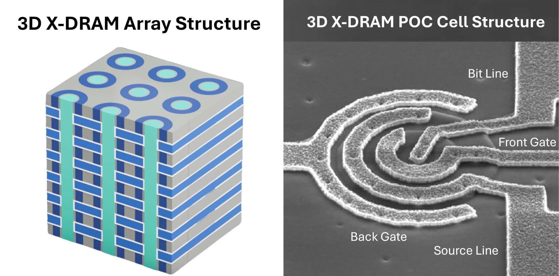
3D X-DRAM™ Breakthrough with POC Test Chip Validation
3D NAND-based process delivering DRAM-class performance, now backed by strategic investment
3D D-DRAM is a game-changing technology. It uses an innovative simple structure like 3D NAND flash memory, making manufacturing and scaling easy and less expensive than other 3D DRAM solutions. Its estimated density is eight times higher than ordinary DRAM.
Unleash AI performance a decade ahead of today’s memory technologies
X-HBM™ delivers breakthrough memory performance for AI chips, servers, and systems, offering up to 16X more bandwidth and 10X higher density than traditional HBM. Built for the growing demands of AI workloads and high-performance computing (HPC), it helps chipmakers and system builders accelerate their roadmaps and unleash new capabilities.
Traditional HBM can’t keep up with rapid GPU advancements, causing memory bottlenecks for AI systems. X-HBM™ solves this with extreme bandwidth and density, enabling faster, more powerful AI chips without waiting for future memory generations.
This innovative 3D memory can accelerate AI Chip performance by 100X and reduce power consumption by 99%. This technology is set to revolutionize the performance, power consumption, and memory density for AI applications like generative AI.
This innovative 3D memory can accelerate AI Chip performance by 100X and reduce power consumption by 99%. This technology is set to revolutionize the performance, power consumption, and memory density for AI applications like generative AI.
August 05, 2025 NEO Semiconductor’s X-HBM™ has been awarded Best of Show for Most Innovative Technology. The X-HBM architecture delivers up to 16X bandwidth for AI chips, eliminating performance bottlenecks in high-performance computing while significantly reducing cost and power consumption. Built on NEO’s breakthrough 3D X-DRAM technology, X-HBM enables direct GPU integration, supports stacking of up to 300 layers, reduces latency, and provides non-volatile AI storage with X-NAND™. This innovation empowers the next generation of AI workloads—from generative AI to edge applications—and exemplifies technologies that are transforming how high-performance memory and storage are designed and deployed. This category recognizes innovations that will change the way high-performance memory or storage works, and which is used in a product.
SANTA CLARA, CA – November 11, 2020 – NEO Semiconductor X-NAND™ was honored with a Flash Memory Summit 2020 “Best of Show” Award for “Most Innovative Startup Company” in the category of Hardware Architecture. X-NAND architecture provides an excellent high-performance solution to lower the cost across all tiers of SSD technologies by increasing the planes of the array without increasing the die size. X-NAND can achieve QLC density with SLC speed.